Power is delivered from board-level components placed far from silicon—dominated by large, bulky inductors, resulting in high losses, large footprint, and limited efficiency. EnaChip’s inductors are thinner and smaller, operate at >10 MHz, and are produced by conventional electroplating.
Integrated magnetics for next-generation power delivery
Compute is no longer limited by logic. It is limited by power.
EnaChip is building integrated magnetic structures that convert voltage at the point of load, with greater efficiency, density and scale.
Embedded magnetics for power delivery at the point-of-load
From discrete power to embedded power to vertical power.
A clear progression from board-level inductors to package integration—and ultimately fully integrated power delivery within the chip stack.
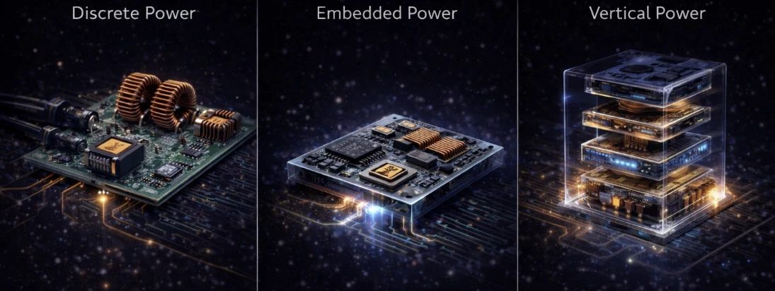
Power moves closer to the chip through package-level integration, improving efficiency but still constrained by packaging complexity and limited scalability. EnaChip enables system designers to bring magnetics into the package alongside PMICs or IVRs.
Power delivery is fully integrated within the chip stack, delivering power directly to silicon for maximum efficiency and performance. EnaChip’s technology scales from discrete to embedded to backside or front-side power delivery.
Power delivery is the primary bottleneck
Power delivery should scale with performance—not limit it.
Compute is no longer limited by logic—it is limited by power. As AI systems scale and advanced packaging compress more performance into smaller footprints, power delivery has emerged as the primary bottleneck. Due to large and bulky power inductors, discrete magnetics consume board space, introduce losses, and limit how closely power can be delivered to silicon. The result is constrained performance, higher energy consumption, and increasing system complexity.
EnaChip addresses this problem at its root. We are developing a new class of power delivery technology based on integrated magnetics, where high-performance magnetic structures are fabricated directly using semiconductor-compatible electroplating processes.
This approach fundamentally changes the ability to integrate higher-efficiency voltage transformers into PMIC or IVR packages—and ultimately within heterogeneous integrated AI modules—more easily and at lower cost.
Manufacturing with electroplating enabling scaling at lower manufacturing cost
Integrating magnetics using electroplating techniques allows devices to be developed in both surface-mount or wire-bonded discrete form, produced at the wafer or panel level, or built directly into laminate package layers. Designers can tune magnetic and insulating layer thickness for specific performance targets while using thick conductor layers to reduce electrical resistance and thermal load.
EnaChip is building the foundation for a new generation of compute infrastructure—where power delivery scales with performance, rather than limiting it.
Backed by semiconductor and deep-tech experts


Powering the systems defining the future
One platform supporting the architectures that need better power delivery most.
EnaChip’s integrated magnetics platform is designed for AI infrastructure, advanced packaging, chiplets, and compact edge systems—where power density, efficiency, and proximity increasingly determine system performance.
AI & Data Centers
Increase compute density while reducing energy usage, power loss, and cooling demand at infrastructure scale.
Advanced Packaging & Chiplets
Enable localized regulation for chiplet and 3D architectures that require power to move closer to the die.
Edge & Compact Systems
Deliver higher-performance power in smaller, lighter, and more efficient form factors where every millimeter matters.
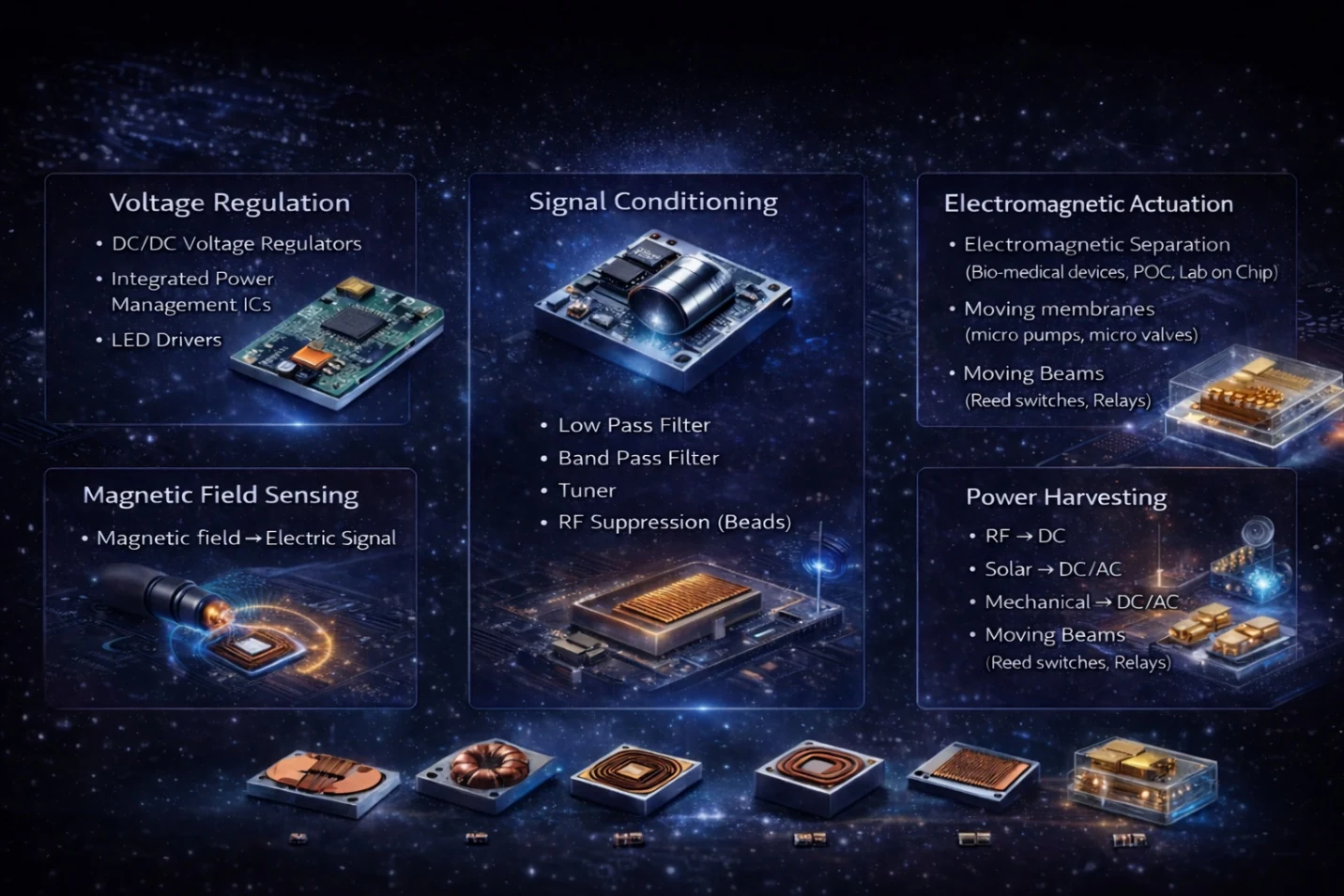
One magnetic platform with system-level reach.
Instead of relying on multiple discrete components, EnaChip enables a unified platform where power, signal, sensing, and actuation can be co-designed and integrated.
Voltage RegulationFiltering & SuppressionMagnetic SensingEnergy HarvestingMicro-Actuation
Built at the intersection of materials, semiconductors, and systems
Leadership built for hard technical problems—and manufacturable outcomes.
Talk to Us
CEO
Mark Popovich
Leading EnaChip’s commercialization of integrated magnetics for next-generation power delivery.

Co-Founder & CTO
Mark Allen
Pioneering microfabricated magnetics and semiconductor process innovation for point-of-load power delivery.

Board / Investor
Anupam Ghildyal
Building and scaling deep-tech companies across semiconductors, manufacturing, materials, and energy.

Board Member
Jim Cable
Guiding growth across semiconductor technology, commercialization, and advanced manufacturing systems.
Mark Popovich is a seasoned semiconductor and advanced materials executive with more than three decades of experience building and scaling technology-driven businesses. He has led companies across the semiconductor packaging, electronic materials, and advanced manufacturing ecosystem, with a strong track record of commercializing new technologies and driving growth at scale.
Most recently, Mark served as CEO of 3D Glass Solutions, where he transformed the company from an R&D-focused startup into a manufacturing and revenue-generating business, raising over $50 million and establishing strategic partnerships with leading industry players including Lockheed Martin, Intel Capital, and Murata. Earlier in his career, Mark held senior leadership roles at Henkel, where he led global electronic materials businesses and corporate venture initiatives, and at Amkor Technology, where he played a key role in expanding global operations and forming strategic joint ventures in semiconductor packaging. He was also a founding member of ChipPAC, helping scale the company through early growth to a successful IPO.
Across his career, Mark has consistently operated at the intersection of materials innovation, semiconductor manufacturing, and system-level integration. At EnaChip, he is leading the company’s effort to bring magnetics into the semiconductor stack—positioning it at the forefront of the next major shift in power delivery and compute architecture.
Mark Allen received undergraduate degrees in chemistry, chemical engineering, and electrical engineering from the University of Pennsylvania (Penn), and the S.M. and Ph.D. degrees from the Massachusetts Institute of Technology. In 1989 he joined the faculty of the School of Electrical Engineering (later ECE) of the Georgia Institute of Technology (GT), ultimately holding the rank of Regents’ Professor and the J.M. Pettit Professorship in Microelectronics. He also served in multiple administrative roles at GT, including Senior Vice Provost for Research and Innovation, and Director of the Institute for Electronics and Nanotechnology (IEN).
In 2013 he returned to Penn to become the Alfred Fitler Moore Professor and Director of Penn’s Singh Center for Nanotechnology. In 2024 he became Chair of Penn’s Department of Electrical and Systems Engineering. Mark’s research is in the area of microelectromechanical systems (MEMS). Beginning with a plenary address to the 1994 IEEE Applied Power Engineering Conference on the topic of integrated inductors, and continuing through today, a major thrust of his program is the realization of microfabricated magnetics for advanced power delivery. He has chaired or co-chaired multiple conferences and co-founded multiple MEMS companies.
Mark is a Fellow of the IEEE, a Fellow of the National Academy of Inventors, and a member of the National Academy of Engineering.
Anupam is a General Partner at Stata Capital and a Venture Partner at Boston Seed Capital. Anupam has been integral in building over ten startups, serving as a co-founder, founding team member, or founding investor across the manufacturing, materials, energy, and technology sectors. He co-founded companies focused on breakthrough innovations including low-cost direct lithium extraction, battery regeneration, and domestic production of rare-earth materials. He was also part of the founding team at VulcanForms.
Anupam has a track record of accelerating early- and growth-stage companies from ideation to full commercialization. He has helped launch over 20 products, raised more than $1 billion in funding, and established manufacturing and sales operations globally.
Jim Cable is a veteran semiconductor executive with more than four decades of experience spanning technology development, commercialization, and company building. He previously served as CEO of Peregrine Semiconductor (now pSemi, a Murata company), where he led the company from early growth through IPO and eventual acquisition, helping establish silicon-on-insulator (SOI) as a foundational technology used in nearly every modern smartphone today.
Jim has held senior leadership roles across the semiconductor ecosystem, including Chief Strategy Officer and Chairman at Finwave Semiconductor, and advisory or board positions at leading technology companies in RF, power, materials, and advanced manufacturing. He brings deep expertise across CMOS, GaN, photonics, and RF systems, along with extensive experience in M&A, venture-backed scaling, and strategic partnerships.
A prolific innovator, Jim is the inventor or co-inventor on more than 100 patents and has authored over 50 technical publications. He holds a PhD in Electrical Engineering from UCLA and is a member of IEEE.
Toward a fully integrated compute stack
Power delivery should scale with performance—not limit it.
EnaChip is building the magnetic layer that allows compute, packaging, and power to be designed as one system—from discrete components to embedded and ultimately vertical integration.